
We design optical thin-film coatings for transmission, reflection and wavelength separation across 0.3–2.5 μm — 300–2500 nm. Our design scope includes anti-reflection coatings, dielectric mirrors, partial reflectors, dichroic coatings and wavelength-selective filters.
We develop the layer structure around the required spectrum, substrate and operating geometry. Material selection, layer thickness, angle of incidence and polarization are considered together with the deposition process used to manufacture the coating.
We can begin with a target transmission or reflection curve, a set of wavelength-specific limits, or spectral data from an existing optic.
Provide the substrate, AOI and polarization conditions with the optical requirement. We use these inputs to define the coating design and the conditions under which it must perform.
If your coating requirement is already defined, send the spectral specification and component drawing for review.
Include the coated surfaces, clear aperture, dimensions, environmental requirements and quantity. Where a prescribed layer stack must be retained, identify the fixed materials and thicknesses.
We support coating development on both newly manufactured optics and customer-supplied substrates. The working range below establishes the starting point for design and manufacturing review.
| Capability | Working Scope | Specification Consideration |
|---|---|---|
| Coating wavelength range | 300–2500 nm | Define the transmission, reflection and rejection intervals |
| Substrate size | 3–480 mm | Geometry and coated surfaces are reviewed with the drawing |
| Coated aperture | Extending to within 1 mm of the edge | Smaller coated areas can be specified where required |
| Substrate supply | Manufactured optics or customer-supplied substrates | Material and surface condition are part of the review |
| Order scale | Prototype through volume production | Quantity informs tooling and production planning |
Coating coverage is defined separately from the physical size of the optic. We review the required aperture, edge exclusions and holder contact areas before establishing the coating configuration.
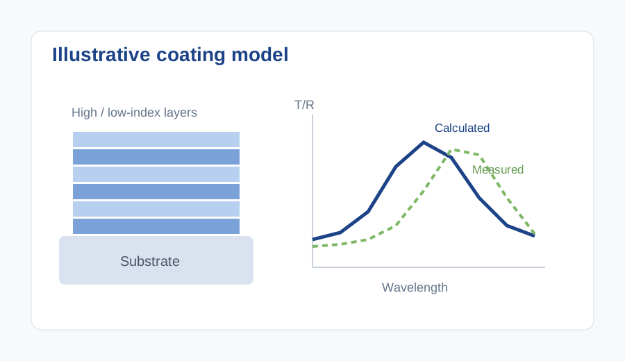
Our design tools include OptiLayer, Film Star and TF Calc for developing and evaluating multilayer coatings. We can also build a coating model around supplied spectral data.
The model connects the optical requirement to material refractive index, layer sequence and thickness. Changing these inputs changes the interference response and the resulting spectrum.
We provide calculated spectral curves during the quotation and development stages. Following manufacture, measured curves and raw spectral data allow the deposited coating to be compared with the design.
The design discussion can therefore address three concrete outputs:
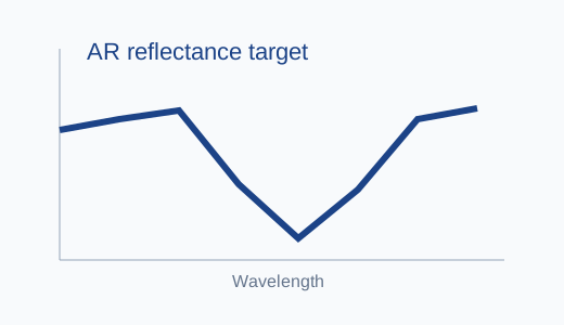
We design single-wavelength, dual-wavelength and broadband AR coatings. On BK7 or fused silica at 0° AOI, specified examples include residual reflectance <0.2% at 1064 nm and <0.15% at 1550 nm.
Broadband configurations include 420–670 nm with residual reflectance <0.5%.
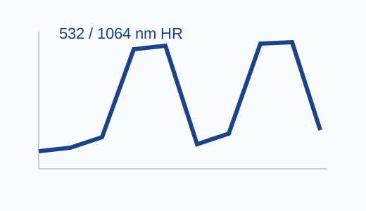
We develop dielectric mirror coatings for single- and dual-wavelength operation.
A dual-wavelength 532/1064 nm configuration specifies reflectance of 99% at 532 nm and 99.5% at 1064 nm. The substrate and selected 0° or 45° operating geometry form part of the coating specification.
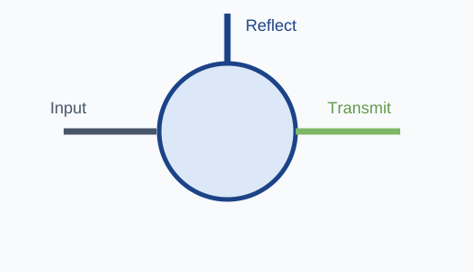
We design partial reflectors with specified reflectance between 10% and 99.7%, selected for the application.
For output couplers and beam splitting, the reflection target is defined together with wavelength, AOI and the required transmitted output. The selected ratio applies to the specified optical condition.
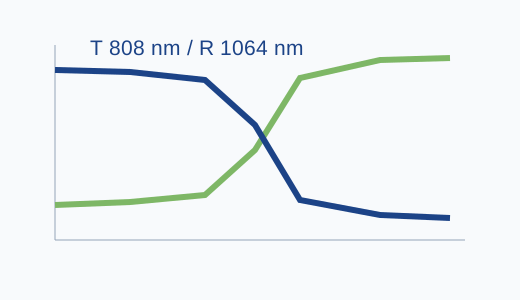
We design dichroic coatings with separate transmission and reflection bands.
One 0° AOI configuration on BK7 or fused silica combines transmission >90% at 808 nm with reflection >99.5% at 1064 nm. Both wavelengths are evaluated as part of the same coating requirement.
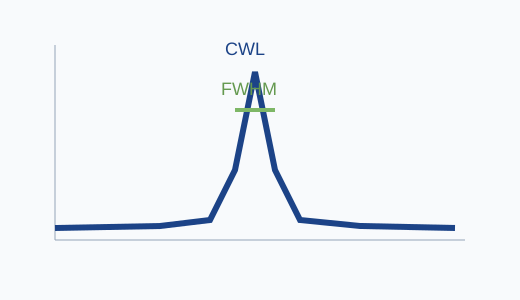
We develop bandpass structures around center wavelength, bandwidth, peak transmission and out-of-band rejection.
For narrowband designs, wavelength tolerance and blocking intervals are defined alongside the passband. The specification examples below show how these requirements are combined.
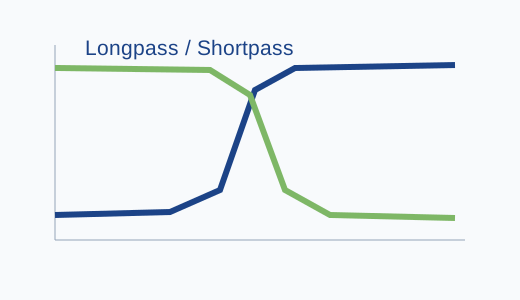
We design edge coatings around the required cut-on or cut-off position, transmission band and rejection band.
Where transmitted and rejected wavelengths are closely spaced, the transition width becomes a central design requirement. We also define the transmission level used to locate the spectral edge.
Our narrowband coating specifications combine wavelength tolerance, bandwidth, transmission and rejection. The following design points illustrate two configurations.
| Center Wavelength | FWHM | Peak Transmission | Blocking OD | Blocking Interval* | Optic Size |
|---|---|---|---|---|---|
| 420 ±0.3 nm | 1 ±0.3 nm | >85% | >4 | 200–800 nm | Ø12.7 × 6 mm |
| 532 ±0.5 nm | 2 ±0.5 nm | >90% | >4 | 200–1100 nm | Ø12.7 × 6 mm |
*Blocking applies outside the transmission band. Passband and transition exclusions must be defined in the individual specification.
For each configuration, the center-wavelength tolerance and bandwidth tolerance are separate requirements. Operating angle and polarization are established during design review rather than inferred from the nominal wavelength.
We match the coating structure to the deposition route, considering the required film properties, layer control and substrate compatibility.
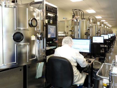
We use electron-beam evaporation for metallic and multilayer dielectric coatings. The source material is evaporated under vacuum and deposited onto the optical surface.
Material selection and layer control are established for the coating being produced.
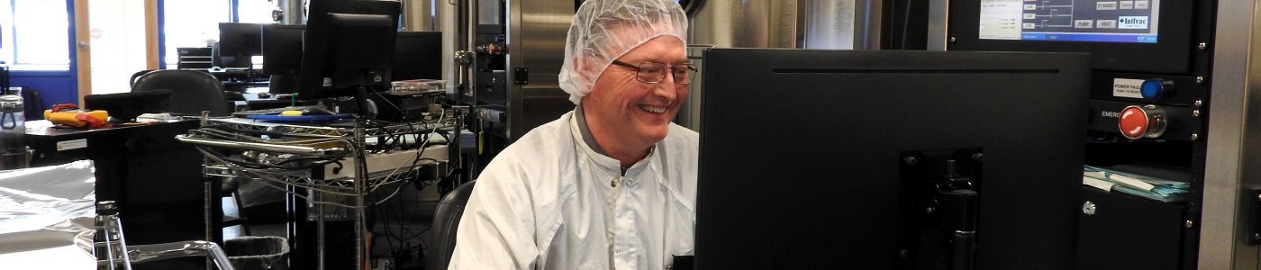
Plasma assistance introduces reactive ions during deposition. We use this route where the coating requirement calls for changes in film properties or adhesion.
The process is selected against the material system and required optical response.
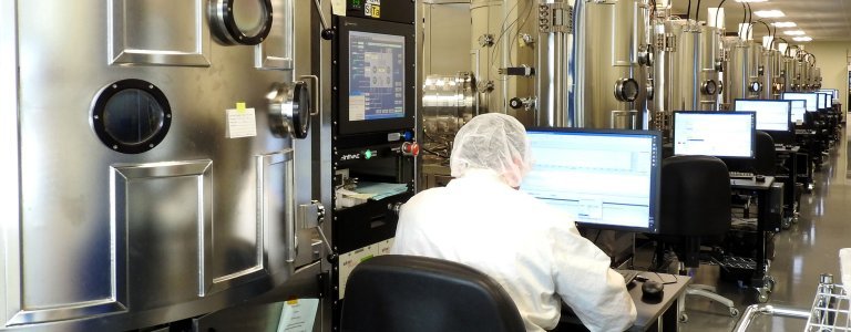
Our thermal evaporation capability supports metallic coatings, including aluminum and silver.
A heat source evaporates the coating material in vacuum. This route provides an established option for reflective coatings where the material and performance requirements suit the process.
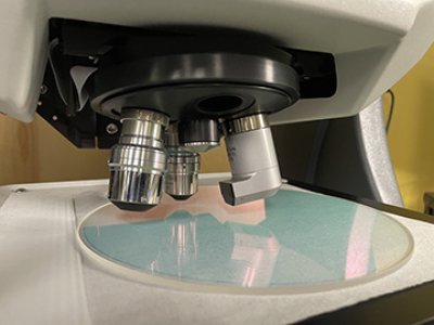
We use IBS for dense thin films requiring precise deposition control. A controlled ion beam sputters material from a target onto the substrate.
The route supports demanding dielectric structures where layer control is central to reproducing the required spectrum.
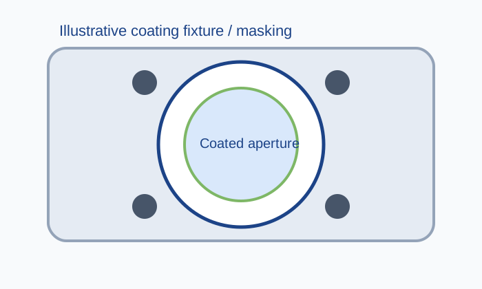
We develop coating fixtures around the actual optic using engineering design and CNC manufacturing. Holder contact, surface access and coating coverage are reviewed together.
Custom masking and counter-rotating uniformity masks support control of the deposited coating across the usable aperture. The fixture must retain the part while leaving the specified optical area accessible.
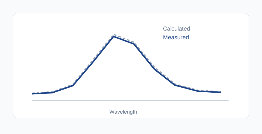
We compare the deposited coating with its calculated transmission and reflection response. The comparison uses the specified wavelength interval, operating angle and polarization condition.
Our spectral testing combines spectrophotometer measurements with laser-based testing for selected optical requirements.
| Measurement Capability | Range or Configuration | Application |
|---|---|---|
| Transmission and reflection | 200–3200 nm, with polarization capability | Spectral comparison with the coating requirement |
| Variable-angle absolute reflection | 10°–70°, using LAMBDA 900 with PELA-1030 | Reflection assessment at specified angles |
| Polarization and phase testing | 632.8 nm He-Ne, S/P configurations | Polarization response and phase-shift difference |
Measured curves and raw data provide the basis for evaluating wavelength position, transmission and reflection. For narrow spectral features, the measurement method and resolution are selected to suit the feature being assessed.
We can start with a target spectrum, an existing specification or spectral data from a reference optic. Send the required transmission, reflection or rejection performance together with the substrate, coated surfaces, clear aperture, AOI and polarization.
Include the required quantity and any environmental or laser operating conditions. If some requirements remain open, identify the fixed limits and the areas where the design can be adjusted.